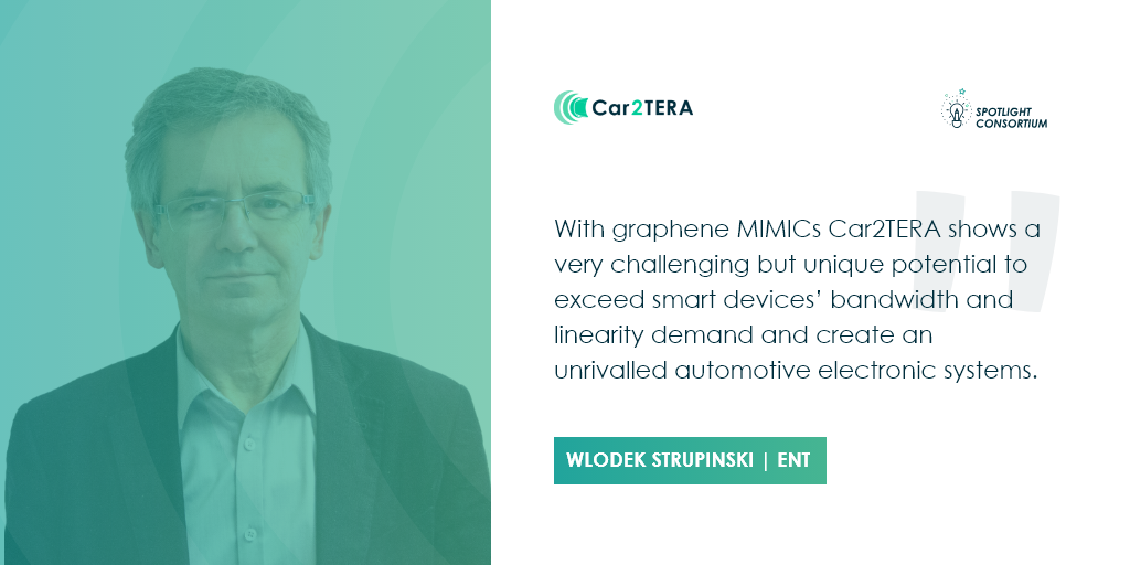
Today in a Talk with Wlodek Strupinski – 5 questions about himself and the Car2TERA H2020 project.
Introduce yourself and tell us a bit about your background.
I am CEO of ENT, a globally recognized semiconductor epitaxy company which is now operating under the VIGO System brand. I am also head of VIGO System’s epitaxy department. The company is involved in works on graphene-based photodetectors . I have more than 30 years’ experience in III-V semiconductor compounds technology for micro- and opto-electronics, silicon carbide compounds for high-power electronics, graphene and other 2D nanomaterials.
I specialise in vapor phase epitaxy and metallorganic vapor phase epitaxy of GaAs-, InP-, GaN-related compounds, SiC and graphene. In 2006 I started the research on graphene growth on SiC, copper, nickel, and other metals. I obtained the world-wide patent for “New method of Graphene growth on SiC”. Since 1994 I have been commercialising the results of research on MOCVD epitaxy by introducing epitaxial wafers of III-V semiconducting compounds onto the global market. I was also the head of Epitaxy dept. at the Institute of Electronic Materials Technology in Warsaw in 1993-2017. Since 2018 I have been a scientist responsible for graphene, hBN and other 2D technologies at Warsaw University of Technology, Physics Dept. partner of EU Graphene Flagship project.
I have been engaged in graphene growth since 2006 being the leader of many research projects’ tasks including EU Graphene Flagship project, Euro Core Project n. 03XP0004A, GRAPHICA Graphene for Integrated Circuit Applications, Project ICT-2013.9.3 FET Young Explorer GRAPHENICS Graphene-enabled on-chip supercontinuum light sources, EUROCORES Programme: EuroGRAPHENE Epitaxial Graphene Transistor (EPIGRAT) Project Number: 09-EuroGRAPHENE-OP-013.
(h-index: 24; number of papers >230; sum of the times cited: 2700).
What is your title and/or role in the project?
I am the leader of WP3 (“Emerging technologies for future THz car sensors and networks “) which aims to use recent achievements in emerging 2D-materials and micromachining THz technologies, to develop groundbreaking technologies for the identified THz applications. This is the first attempt of using graphene-based electronics for communication and sensing applications above 100GHz; and graphene circuits would offer real advantages for the targeted applications. This is a direct exploitation of latest results of the Graphene Flagship Programme towards an industrial-level demonstrator. Graphene MMICs according to the results achieved at Chalmers Univ., so far only attempted below 100 GHz, have shown extraordinary linearity, as compared to semiconductor circuits. This project requires very large bandwidths (100 GHz) and therefore would highly benefit from the linearity of graphene field-effect transistors. My role is to coordinate the works within WP3, and after its completion I am responsible for the cooperation of the activities performed within WP1,8,9 which involve the development of technological specifications to guarantee a well-structured technical implementation of the project, application of graphene, and later for the results dissemination. I am also taking part in the operational management of the project
What are your contributions to the project? (Specify what deliverables and/or tasks you are responsible for)
In this project we will demonstrate the potential of graphene to be used in handling very demanding signals at frequencies not yet investigated, namely D-band 110-170 GHz and G-band 140-220 GHz. My main task in the project is to fabricate and characterise high quality graphene on SiC and other substrates including sapphire, SiO2 and other 2D materials as hBN, with high transport parameters, repeatability and uniformity, as required by sub-THz devices, developed in WP3. Various protocols of graphene growth and transfer onto arbitrary substrates will be verified towards high device performance and the industrial implementation. This will provide significant advance over existing sub-THz technologies operating at millimetre wave (mm-wave) frequencies. The devices are to be applied in the project´s system demonstrators realized within WP5 and WP6.
What challenges can you foresee in the project?
The key challenge is to develop high quality graphene with such parameters and technological solutions that would satisfy the requirements of sub-THz devices i.e. MMIC-grade uniformity, OFF/ON ratio of channel resistance >> 5, accurate nonlinear device models, MMIC-processing, interfacing with Si THz-platform and that would later result in the creation of the economically and commercially viable product. If the emerging technologies can be successfully implemented in laboratory, the demonstrators will utilize them to achieve outstanding performance targeting real-world applications.
How do you think the project outcome could affect our daily life?
With alarming figures of annual road fatalities worldwide, safety has become a key issue for the whole automotive industry. Car radar sensors are now a vital part of any modern automobile design, enabling greater degree of vehicle automation. They provide to the driver accurate and reliable information on the car surroundings in the most effective and least distractive manners, allowing the control unit to take preventative or corrective actions. They are fundamental in helping car manufacturers to produce models that are safer, more fuel efficient and more comfortable to drive. Application of graphene can significantly contribute to increasing sensors capabilities and thus the development of safer and more reliable systems. Apart from application in sensors, graphene is an attractive material to be used in order to increase data transfer not only in cars but in many areas of our daily life.
