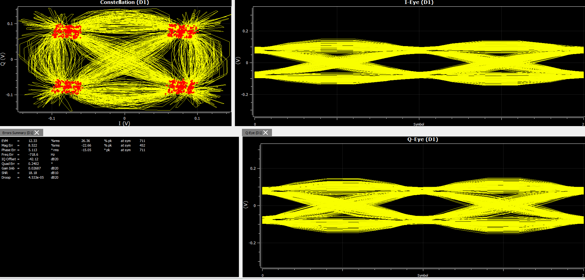
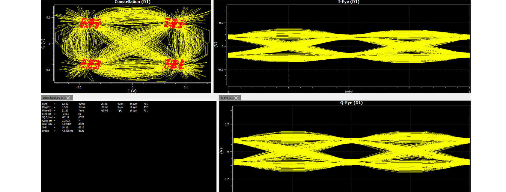
There are some huge differences between the daily development process for a typical semiconductor products and R&D projects with a high degree of innovation. While in a standard development with qualified and released technologies a full characterization plan has to be fixed before the design starts there is a lot of research activities necessary in forefront projects beside the design, layout, packaging and lab-preparation work. One important activity is “pre-silicon verification” this means extensive “virtual” testing with system simulation using actual results from circuit simulations, testchips and other projects to have a clear expectation on the IC performance before the system evaluation starts. This includes the simulation of complex modulation schemes, integration of 3D EM Simulation and the influence of fiber and coupler characteristics in worst-case configurations, the results are so called “eye diagrams”, which give you a clear picture of the margins of the setup.
Especially for sub-Terahertz developments in new technologies with the very complex active and passive devices this is a key to shorter development cycles (and reduced costs).
In parallel the Backend processing and the eWLB packaging is ongoing to deliver the latest samples. So open the eyes and you will see.

